LED packaging technology and structure has a lead, power-based packaging, SMD (SMD), on-board chip directly loaded (COB) four stages.
(1) Pin type (Lamp) LED package
LED foot-type package with lead frame for a variety of packaging appearance of the pin, is the first successful development of the market put the packaging structure, a wide variety of products, high technology maturity, the package structure and reflective layer is still improving. Commonly used 3 ~ 5mm package structure, generally used for small current (20 ~ 30mA), low power (less than 0.1W) LED package. Mainly used for instrument display or instructions, large-scale integration can also be used as a display. The disadvantage is that the package thermal resistance (generally higher than 100K / W), shorter life.
(2) Power LED package
LED chip and package to the direction of high-power development, in the large current than Φ5mmLED 10 ~ 20 times the luminous flux, must be effective cooling and non-deterioration of the packaging material to solve the problem of light failure, so the shell and package is the key Technology, can withstand the number of W power LED package has emerged. 5W series of white, green, blue and green, blue power LED from the beginning of 2003 supply, white LED light output up to 1871m, luminous effect of 44.31 lm / W green light problem, developed to withstand 10W power LED, Tube; size 2.5mm X2.5mm, can work in the 5A current, light output of 2001 lm, as a solid light source has a lot of room for development.
(3) surface assembly (SMD) type (SMD) LED package
As early as 2002, the surface mount package of LED (SMDLED) gradually accepted by the market, and get a certain market share from the pin package to SMD in line with the development trend of the electronics industry, many manufacturers to launch such products.
SMDLED is the highest market share of LED packaging structure, this LED packaging structure using the injection process will be wrapped in the metal lead frame in the PPA plastic, and the formation of a specific shape of the reflective cup, the metal lead frame from the bottom of the reflective cup extends to the device side , Through the outward flat or inward bending to form the device pin. Improved SMDLED structure is accompanied by white LED lighting technology, in order to increase the use of a single LED device power to improve the brightness of the device, engineers began to find ways to reduce the SMDLED thermal resistance, and the introduction of the concept of heat sink. This improved structure reduces the height of the initial SMDLED structure. The metal lead frame is placed directly on the bottom of the LED device. A reflective cup is formed around the metal frame by injection of plastic. The chip is placed on top of the metal frame. The metal frame is directly welded to the Circuit board, the formation of vertical cooling channel. As the development of materials technology, SMD packaging technology has overcome the heat, life and other early problems, can be used to package 1 ~ 3W high-power white LED chip.
(4) COB-LED package
COB package can be more than one chip directly packaged in the metal-based printed circuit board MCPCB, through the substrate directly heat, not only can reduce the stent manufacturing process and its cost, but also has the advantage of reducing thermal resistance. The PCB board may be a low cost FR-4 material (glass fiber reinforced epoxy), or it may be a high thermal conductivity metal or ceramic matrix composite material such as an aluminum substrate or a copper clad ceramic substrate. The wire bonding can be used under high temperature thermal ultrasound bonding (gold ball welding) and ultrasonic bonding at room temperature (aluminum split knife welding). COB technology is mainly used for high-power multi-chip array LED package, compared with the SMD, not only greatly improve the package power density, and reduce the package thermal resistance (usually 6-12W / m · K).
From the cost and application point of view, COB will become the future direction of the mainstream lighting design. COB package LED module in the floor to install a number of LED chips, the use of multiple chips can not only improve the brightness, but also help to achieve a reasonable LED chip configuration, reduce the input power of a single LED chip to ensure high efficiency. And this surface light source to a large extent to expand the cooling area of the package, so that heat is easier to conduct to the shell. The traditional LED lighting practices are: LED light source discrete devices - MDCB light source module - LED lamps, mainly based on the core light source components are not applicable to the practice, not only time-consuming, and high cost. In fact, if you take the "COB light module-LED lighting" route, not only save time and effort, and can save the cost of device packaging.
In short, whether it is a single device package or modular COB package, from small power to high power, LED package structure design around how to reduce the device thermal resistance, improve the light effect and improve reliability and expand.
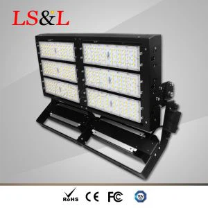
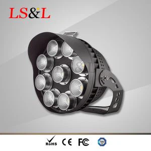
Hot products: motion sensor linear lamp,150W power high bay,tri-proof LED lamp,LED Mining lamp,120cm linear high bay,LED grow lamp